- 您现在的位置:买卖IC网 > Sheet目录3873 > PIC16F886-I/ML (Microchip Technology)IC PIC MCU FLASH 8KX14 28QFN
2009 Microchip Technology Inc.
DS80302F-page 5
PIC16F88X
3.
Module: Analog-To-Digital Converter
(ADC) Module
Selecting the VP6 reference as the analog input
source
(CHS<3:0> = 1111)
for
the
ADC
conversion after sampling another analog channel
with input voltages approximately greater than
3.6V can temporarily disturb the HFINTOSC
oscillator.
Work around
Select an ADC channel with input voltages lower
than 3.6V prior to selecting the VP6 reference
voltage input. Any analog channel can be used,
even if that channel is configured as a digital I/O
(configured as an output) that is driving the output
pin low. An alternative is to configure the CVREF
module to output a voltage less than 3.6V and then
selecting that analog channel CHS<3:0> = 1110
as the analog input source.
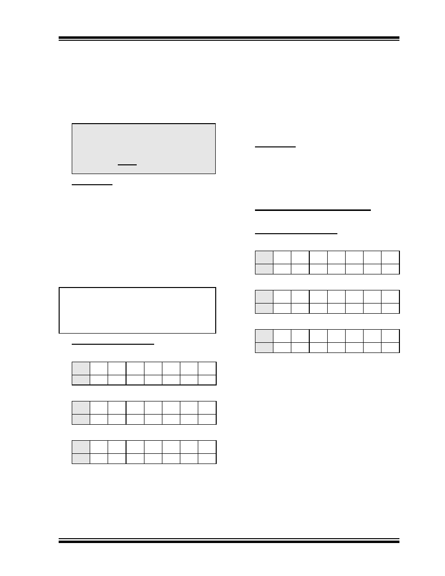
EXAMPLE 2:
AVOID DISTURBING THE
HFINTOSC OSCILLATOR
Affected Silicon Revisions
PIC16F882
PIC16F883/PIC16F884
PIC16F886/PIC16F887
4.
Module: MSSP (SPI Master Mode)
With MSSP in SPI Master mode, FOSC/64 or
Timer2/2 clock rate and CKE = 0, a write collision
may occur if SSPBUF is loaded immediately after
the transfer is complete. A delay may be required
after the MSSP Interrupt Flag bit, SSPIF, is set or
the Buffer Full bit, BF, is set and before writing
SSPBUF. If the delay is insufficiently short, a write
collision may occur as indicated by the WCOL bit
being set.
Work around
Add a software delay of one SCK period after
detecting the completed transfer and prior to
updating the SSPBUF contents. Verify the WCOL
bit is clear after writing SSPBUF. If the WCOL is
set, clear the bit in software and rewrite the
SSPBUF register.
Date Codes that pertain to this issue:
All engineering and production devices.
Affected Silicon Revisions
PIC16F882
PIC16F883/PIC16F884
PIC16F886/PIC16F887
Note:
This only occurs when selecting the
VP6 reference ADC channel using the
CHS<3:0>
bits
in
the
ADCON0
register and NOT during the start of an
actual ADC conversion using the
GO/DONE bit in the ADCON0 register.
A0
X
A0
X
A2
X
BANKSEL
ADCON0
;
MOVLW
B’XX111001’
;Select ADC
MOVWF
ADCON0
;Channel CVREF
MOVLW
B’XX111101’
;Select ADC
MOVWF
ADCON0
;Channel VP6
A0
X
A0
X
A2
X
发布紧急采购,3分钟左右您将得到回复。
相关PDF资料
PIC24F08KA101-I/SO
IC PIC MCU FLASH 8K 20-SOIC
PIC18F44J10-I/P
IC PIC MCU FLASH 8KX16 40DIP
PIC18LF45J10-I/PT
IC PIC MCU FLASH 16KX16 44TQFP
DSPIC30F6015T-20I/PT
IC DSPIC MCU/DSP 144K 64TQFP
DSPIC30F6014AT-20I/PT
IC DSPIC MCU/DSP 144K 80TQFP
PIC24F16KA102-I/SS
IC PIC MCU FLASH 16K 28-SSOP
DSPIC30F6013AT-20I/PT
IC DSPIC MCU/DSP 132K 80TQFP
DSPIC30F6012AT-20I/PT
IC DSPIC MCU/DSP 144K 64TQFP
相关代理商/技术参数
PIC16F886-I/ML
制造商:Microchip Technology Inc 功能描述:8-Bit Microcontroller IC
PIC16F886-I/SO
功能描述:8位微控制器 -MCU 14KB Flash 368 RAM 25 I/O RoHS:否 制造商:Silicon Labs 核心:8051 处理器系列:C8051F39x 数据总线宽度:8 bit 最大时钟频率:50 MHz 程序存储器大小:16 KB 数据 RAM 大小:1 KB 片上 ADC:Yes 工作电源电压:1.8 V to 3.6 V 工作温度范围:- 40 C to + 105 C 封装 / 箱体:QFN-20 安装风格:SMD/SMT
PIC16F886-I/SO
制造商:Microchip Technology Inc 功能描述:8-Bit Microcontroller IC
PIC16F886-I/SP
功能描述:8位微控制器 -MCU 14KB Flash 368 RAM 25 I/O RoHS:否 制造商:Silicon Labs 核心:8051 处理器系列:C8051F39x 数据总线宽度:8 bit 最大时钟频率:50 MHz 程序存储器大小:16 KB 数据 RAM 大小:1 KB 片上 ADC:Yes 工作电源电压:1.8 V to 3.6 V 工作温度范围:- 40 C to + 105 C 封装 / 箱体:QFN-20 安装风格:SMD/SMT
PIC16F886-I/SP
制造商:Microchip Technology Inc 功能描述:8-Bit Microcontroller IC
PIC16F886-I/SS
功能描述:8位微控制器 -MCU 14KB Flash 368 RAM 25 I/O RoHS:否 制造商:Silicon Labs 核心:8051 处理器系列:C8051F39x 数据总线宽度:8 bit 最大时钟频率:50 MHz 程序存储器大小:16 KB 数据 RAM 大小:1 KB 片上 ADC:Yes 工作电源电压:1.8 V to 3.6 V 工作温度范围:- 40 C to + 105 C 封装 / 箱体:QFN-20 安装风格:SMD/SMT
PIC16F886-I/SS
制造商:Microchip Technology Inc 功能描述:8-BIT MICROCONTROLLER IC
PIC16F886T-E/ML
制造商:Microchip Technology Inc 功能描述: